The semiconductor industry is evolving rapidly, and with each passing year, chip designs are becoming more complex. To keep up with this increasing complexity, engineers need more innovative tools that can help them speed up design processes without sacrificing performance, power efficiency, or reliability. This is where Large Language Models (LLMs) come into play. These AI-driven models are reshaping how engineers approach chip design, not by replacing human creativity but by offering powerful assistance throughout the design process.
In this edition of the Semiconductor And Beyond Newsletter, let us dive into how LLMs impact chip design workflows, from automating the generation of hardware description languages to optimizing layouts and improving verification processes.
For decades, Electronic Design Automation (EDA) tools have served as the foundation of chip design. However, the emergence of LLMs is transforming the way engineers engage with these tools. Instead of meticulously adjusting each design parameter, engineers can now leverage LLM-powered systems like ChatEDA to interact with their design tools through natural language. This shift enables a more intuitive and user-friendly experience, allowing engineers to concentrate on higher-level design challenges while the AI takes over routine tasks such as script generation and layout optimization.
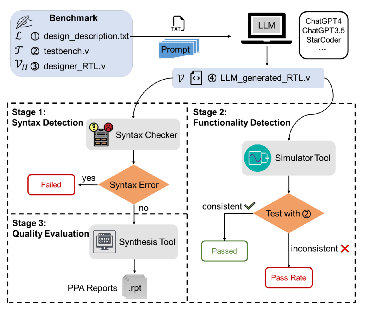
This transformation extends beyond tool interaction to the code that drives chip design. Writing HDL (Hardware Description Language) code has traditionally been tedious and time-consuming, requiring meticulous attention to detail. With LLMs like ChipGPT and RTLLM, this task is even automated. Engineers can input design specifications, and these advanced models will generate RTL code along with the necessary EDA control scripts. In addition to automating code generation, these tools assist in evaluating the code’s quality, checking for syntax errors, ensuring functionality, and optimizing critical metrics like Power, Performance, and Area (PPA). This significantly reduces the manual workload, allowing engineers to shift their focus toward refining and innovating design concepts rather than spending time coding from scratch.
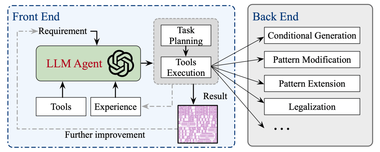
Placement and layout are also critical in determining a chip's performance and power efficiency. Traditionally, this involves long hours of trial and error. However, with models like ChipNeMo, engineers can automatically optimize component placement, leading to more efficient designs in significantly less time. Tools like ChatPattern enable layout customization through simple natural language inputs, allowing engineers to quickly iterate on designs without being bogged down in the finer details of layout planning. This efficiency in layout planning saves valuable time for engineers.
Verification is another area where LLMs are making a big difference. Tools like VeriGen and AssertLLM are used to generate verification assertions and test benches, which help catch errors early in the design process. This early detection of issues provides engineers with a sense of security, as it can save significant time and cost later on. By automating these tasks, LLMs reduce the need for manual verification and allow engineers to ensure their designs meet functional and performance criteria before moving forward.
With the increasing complexity of chip designs, the risk of security vulnerabilities also rises. LLMs are at the forefront of addressing this challenge by providing robust tools for hardware security verification. For instance, LLM4SecHW and RTLFixer are specifically designed to proactively identify and correct hardware vulnerabilities. These models are focused on early detection of bugs and security issues that could otherwise remain undetected until much later in the design process, thereby saving time and reducing risk.
While LLMs have shown great success in digital chip design, the move toward analog and mixed-signal design is still in the early stages. However, tools like AnalogCoder and SynthAI pave the way for AI-driven automation in this domain. These tools are expected to streamline tasks like analog layout generation and signal integrity optimization, which have traditionally been more challenging to automate. As LLMs evolve, they will likely play a more significant role in optimizing analog circuits alongside their digital counterparts.
As we look ahead, it is clear that LLMs will continue to be a major force in transforming EDA tools. Platforms like Synopsys DSO.ai and Cadence Cerebrus already lead the charge by integrating AI for real-time, multi-parameter optimization. These tools are making it possible to optimize chips for power, performance, area, and cost simultaneously. We can expect these AI-augmented platforms to cover the entire design lifecycle, from the initial RTL generation to the final tape-out, giving engineers a more streamlined and efficient process.
LLMs are also quickly becoming an essential part of the chip design toolkit. They help engineers handle repetitive, data-heavy tasks like generating HDL code, optimizing layouts, and verifying designs. But it is important to remember that these tools are here to assist, not replace. Human creativity and insight remain critical in making the high-level decisions that drive innovation. LLMs allow engineers to work more efficiently and focus on what they do best - solving complex problems and pushing the boundaries of what’s possible in semiconductor design.
Below is a curated list of various LLM approaches proposed in academic research, each designed to enhance different aspects of semiconductor chip design. These models explain how traditional workflows will evolve by automating tasks such as RTL generation, layout optimization, verification, and even hardware security.
ChipNeMo: Domain-adapted LLM designed to optimize chip design workflows by leveraging GPT models for placement and layout optimization.
ChatEDA: An LLM-powered autonomous agent that interacts with engineers in natural language to assist with EDA tasks.
ChipGPT: Explores natural language-based hardware design and automates HDL code generation.
RTLLM: Open-source LLM focused on generating RTL code and benchmarking design performance.
RapidGPT: Automates HDL design as a pair-designer, streamlining hardware language generation.
AutoChip: Provides LLM feedback for refining HDL generation and optimizing hardware design.
VeriGen: Automates Verilog code generation, enabling faster design and verification processes.
AssertLLM: Assists in generating and evaluating hardware verification assertions from design specifications.
GPT4AIGChip: Utilizes LLMs to automate AI accelerator design and improve chip performance.
RTLFixer: Automatically fixes RTL syntax errors using LLM-based models, speeding up verification.
Cynthia: Multi-agent generative AI framework for automated modular HLS design and optimization.
AnalogCoder: Focuses on analog circuit design through training-free code generation, simplifying complex designs.
CodeGen: Open-source LLM that facilitates multi-turn program synthesis and HDL script generation.
ChatPattern: Uses LLMs for layout pattern customization via natural language inputs.
VerilogEval: Evaluates LLM-generated Verilog code to ensure correctness, efficiency, and performance.
LLM4SecHW: Leverages domain-specific LLMs to enhance hardware security debugging and verification.
DIVAS: End-to-end LLM framework for SoC security analysis and protection during the design phase.
EDA Corpus: A dataset LLMs use to enhance interaction with OpenROAD, improving EDA workflows.
RTLCoder: Outperforms GPT-3.5 in RTL code generation, using open-source datasets for better design results.
LayoutCopilot: LLM-powered multi-agent framework for collaborative analog layout design.
Together, these approaches certainly demonstrate how LLMs are driving innovation in the chip design process, simplifying complex tasks, and opening new possibilities for efficiency and performance across all stages of hardware development.
In all, the future of chip design is promising, with AI emerging as a transformative force. Large Language Models (LLMs) lead this revolution, acting as indispensable partners to engineers rather than mere tools. As these silicon design focused AI-driven models evolve further, they will unlock unprecedented efficiency, precision, and innovation across digital and analog chip design.
CONNECT
Whether you are a student with the goal to enter semiconductor industry (or even academia) or a semiconductor professional or someone looking to learn more about the ins and outs of the semiconductor industry, please do reach out to me.
Let us together explore the world of semiconductor and the endless opportunities:
And, do explore the 200+ semiconductor-focused blogs on my website.


