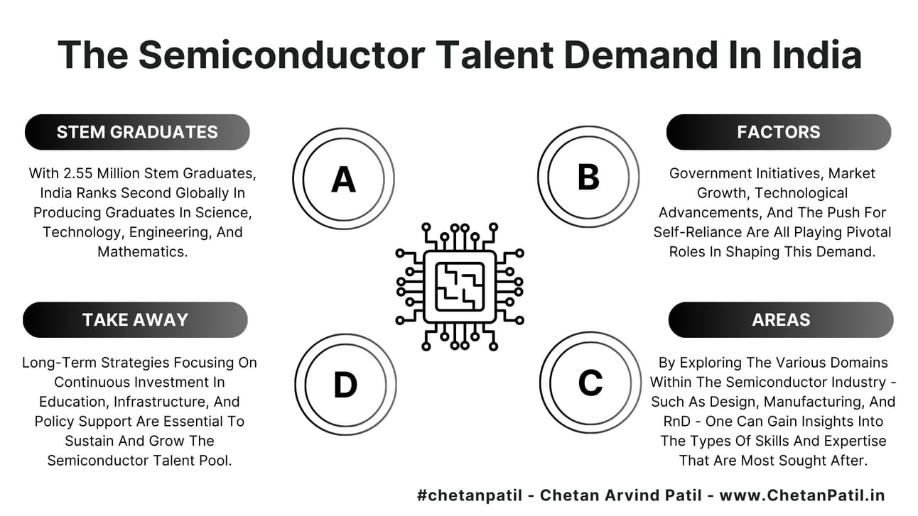
India's semiconductor industry is on the cusp of a significant transformation, driven by a huge demand for talent and rapid technological advancements. With 2.55 million STEM graduates yearly, India ranks second globally in producing Science, Technology, Engineering, and Mathematics graduates.
As the world increasingly relies on semiconductors for everything from smartphones to electric vehicles, India's role as a key player in this global ecosystem becomes increasingly critical.
Read more....

THREAD
The Semiconductor CMM Article SoW:
Published "Beyond Moore - Design And Manufacturing Challenges In System-On-A-Wafer" in CMM Magazine, this article delves into the design and manufacturing challenges of System-On-A-Wafer (SoW) technologies. Unlike traditional SoC or SiP designs, SoW integrates multiple functional dies onto a single wafer, offering higher performance and efficiency.

The Semiconductor LLM And Manufacturing:
Large Language Models (LLMs) are revolutionizing semiconductor manufacturing with advanced NLP capabilities, facilitating complex data analysis, predictive maintenance, and process optimization. LLMs improve yield rates, reduce defects, and enhance efficiency in semiconductor fabrication. They also aid in predictive equipment maintenance and optimize Electronic Design Automation (EDA) processes, streamlining supply chain management.

The Semiconductor In-House Auto Semi:
The global chip shortage has prompted automakers to move semiconductor design and manufacturing in-house, developing custom chips for features like autonomous driving and ADAS. This shift reduces dependency on suppliers, mitigates price volatility, and supports the integration of specialized semiconductors for EVs and autonomous systems, enhancing innovation and competitiveness.

The Semiconductor India Talent Demand:
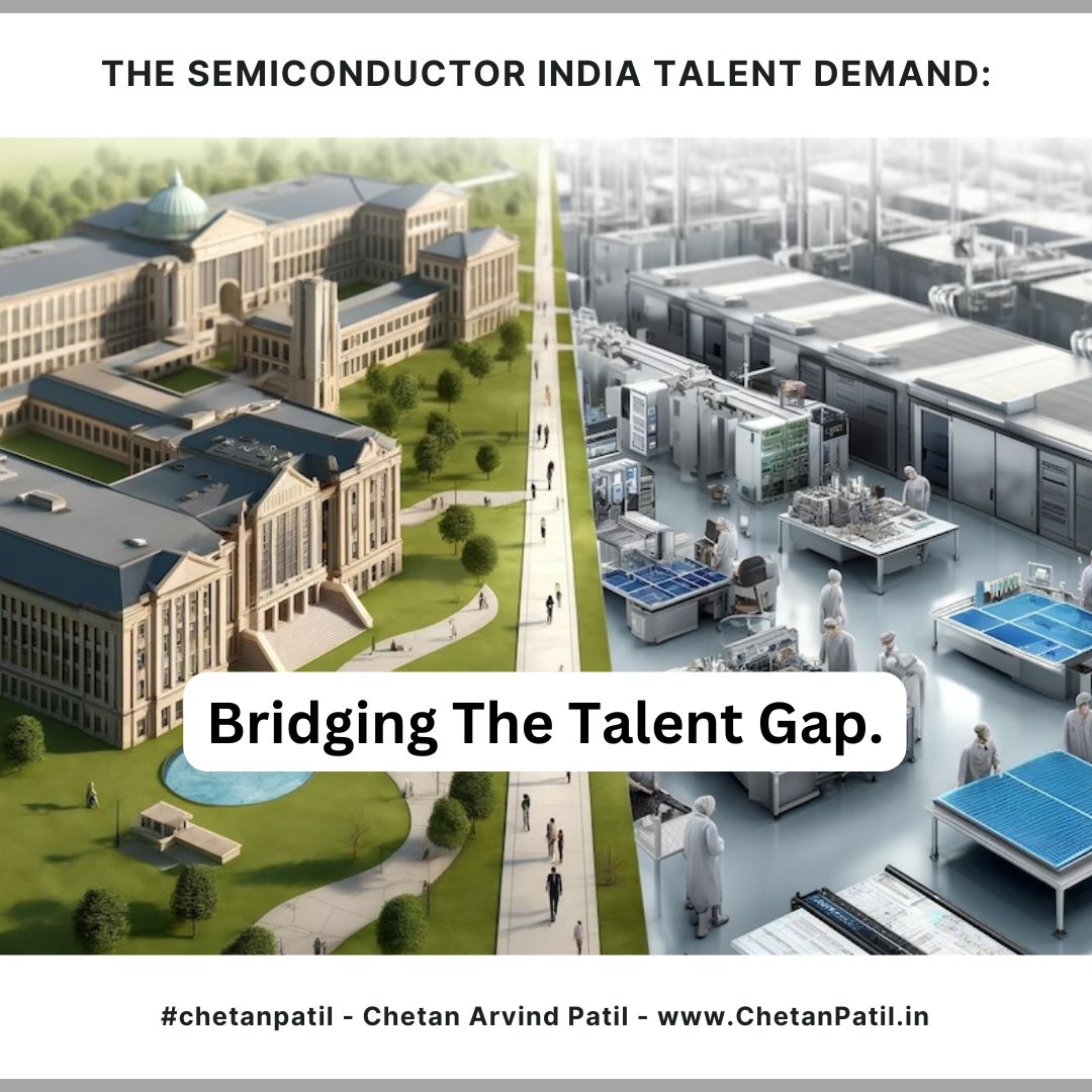
India's semiconductor industry estimates a need for 275,000 professionals in chip design, 25,000 in fabrication, and 29,000 in ATMP facilities over the next decade. Despite producing over a million engineering graduates annually, there is a significant skill gap. Government initiatives and specialized training programs aim to build a skilled workforce, leveraging India's demographic advantage and emphasis on STEM education.

The Semiconductor Future FAB Count:
By 2030, the semiconductor industry is expected to see a significant increase in fabs, potentially reaching 1,000. Notable investments include TSMC's partnerships in Japan, South Korea's $471 billion plan, and the Chips Act-driven projects in the US and Europe. Emerging markets like India, supported by government incentives, are also becoming key players in semiconductor manufacturing.

VLOG
In this week's video, I delve into the booming demand for semiconductor talent in India. As the semiconductor industry, vital to our modern technology, grows exponentially, India emerges as a critical player, with its market expected to reach USD 64 billion by 2026. Despite a rich history and substantial investments, there is a significant skill gap in both design and manufacturing.
With advancements in AI and a projected VLSI market growth, the demand for skilled professionals is higher than ever. I explore how India's educational infrastructure and government initiatives are gearing up to meet this demand and the immense career opportunities this presents.
GOVERNMENT
Malaysia's National Semiconductor Strategy (NSS) is a welcome move, but faces challenges in its talent pool. Despite aiming to become a global R&D hub, the NSS needs to address the current shortage of highly skilled domestic engineers. To compete effectively, the strategy should prioritize subsidizing IC design houses, a higher-margin sector, while simultaneously expediting work visas and residency permits for foreign engineers. This dual focus on domestic talent development and global recruitment is crucial for Malaysia to climb the semiconductor value chain.
INDUSTRY
Semiconductor foundry VIS and chipmaker NXP are teaming up to build a new $7.8 billion 300mm wafer fabrication facility (fab) in Singapore. VIS will operate the fab, focusing on 130nm to 40nm process technologies for automotive, industrial, consumer, and mobile applications. Construction is expected to begin later in 2024, with initial production targeted for 2027. The joint venture, named VisionPower Semiconductor Manufacturing Company (VSMC), aims to produce 55,000 wafers monthly by 2029 and create 1,500 jobs in Singapore. This collaboration strengthens Singapore's position in the global semiconductor ecosystem.
Rocket Lab, an IoT satellite and connectivity provider, secured preliminary approval for up to $23.9 million from the US Chips and Science Act. This funding will modernize their New Mexico facility and boost the production of space-grade compound semiconductors by 50% over three years. Notably, Rocket Lab, through its SolAero acquisition, is a major US player in this critical space technology, supplying solar cells for missions like James Webb and Ingenuity Mars Helicopter. This partnership with the Department of Commerce strengthens US capabilities in a competitive global market.
Alphawave Semi and Samsung Foundry solidify their partnership to tackle next-gen chiplet development for high-performance computing (HPC). This alliance expands access to Alphawave's cutting-edge IP for PCI Express 7.0, high-speed Ethernet, and UCIe standards, all optimized for Samsung's 5nm, 4nm, and 2nm processes. This empowers designers with the tools to build high-performance chiplets for AI, HPC, and more. Both companies view this as a major step forward in high-speed connectivity and HPC advancements.
ACADEMIA
AST's CHIPS Act contract win highlights academia's crucial role. By fostering collaboration between industry (AST) and academic institutions, this research initiative aims to propel advancements in chip fabrication, materials, and manufacturing. This focus on academia aligns with the CHIPS Act's goal of reigniting US leadership in semiconductor technology through cutting-edge research.
RESEARCH
Diamond Quanta's new co-doping method tackles inefficiencies in diamond semiconductors, boosting performance and power handling. This research, detailed in upcoming publications, improves charge transport and enables efficient quantum gates for future computers. Their cost-effective approach avoids limitations of traditional methods, making diamonds a viable option for high-power applications in AI, automotive, and aerospace industries. This research positions Diamond Quanta as a leader, offering a powerful and efficient alternative to silicon-based semiconductors.
TOOLS
OpenTimer is an advanced timing analysis solution designed for professional integrated circuit (IC) design workflows. This tool empowers IC designers with interactive analysis capabilities to ensure circuit timing meets specifications. It offers flexibility by supporting both path-based and graph-based analysis approaches. This innovative tool stands out for its compatibility with industry-standard file formats, including .lib, .v, .spef, and .sdc.
JOBS AND CAREER
ChipIN Centre invites nominations for a 6-month internship at Intel from the participating institutions under the C2S Prog.
Area of internship: VLSI Design and Embedded Software
Last Date: June 17, 2024
Image Credit: Digital India Programme
CONNECT
Whether you are a student with the goal to enter semiconductor industry (or even academia) or a semiconductor professional or someone looking to learn more about the ins and outs of the semiconductor industry, please do reach out to me.
Let us together explore the world of semiconductor and the endless opportunities:
Website: https://www.ChetanPatil.in
Twitter: https://twitter.com/iChetanPatil
Instagram: https://www.instagram.com/ChetanArvindPatil

