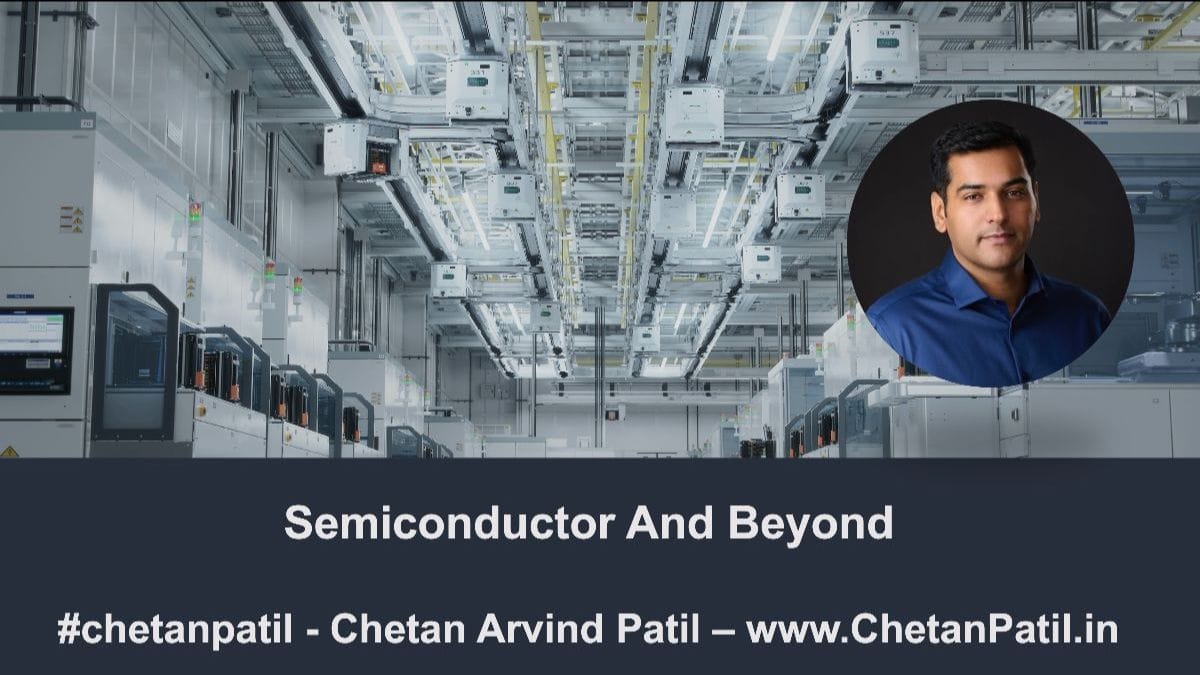
In the last blog post, I wrote about a guide students can use while selecting a principal focusing on joining the semiconductor industry as an engineer. As an extension to that blog, I am now writing about another guide that students can use to match the skills they have (or believe they will acquire on the go) with the specific functions of the semiconductor industry.
Read more....

THREAD
If you are a student or even a professional looking to switch a job, then networking is the right approach. Do read this thread I wrote to summarize different ways in which students can acquire new jobs.
A paper title "High-Speed Emerging Memories For AI Hardware Accelerators," was published in the Nature. Read and learn about what this paper summarizes and how it can be used by researchers (and designers) to better their AI accelerators.
GPUs are at the forefront of AI computing and a recent report from UBS states that the GM% could be as high as 80%. Which is certainly a surprise and also goes on to show the demand that customers are willing to pay such a high cost. Learn more about this on my post on LinkedIn.
AI Infra is going to be a game changer and the focus will be on create network of AI Centers and AI Edge solutions. Read and learn more about AI Infra.
AI in semiconductor industry, specifically manufacturing, is not new. There are several use cases that exists and more unique case will come up as AI evolves into AGI and ASI.
VLOG
Watching this insightful video to capture quick details about how AI is going to change semiconductor design while it is also AI use cases for manufacturing of semiconductors.
GOVERNMENT
South Korea to forge the world's largest semiconductor hub by 2047. The plan will transform Gyeonggi Province into a mega chip cluster, boasting 16 new fabs and generating an estimated 3 million jobs. Slated to produce 7.7 million wafers monthly by 2030, this industrial titan aims to seize 10 percent of the worldwide system semiconductor market. The mega chip cluster is poised to be more than a manufacturing powerhouse; it’s a job creation engine. The construction phase alone will create 70,000 jobs, with the ripple effect expected to generate employment for 3.46 million people.
Indian Government approves semiconductor MoU with EU. India’s Union Cabinet, chaired by Prime Minister Modi, has approved the Memorandum of Understanding (MoU) on semiconductors signed by India and the European Union in November 2023. The agreement sets out how the two governments will work together to build a robust semiconductor supply chain and further technological advancements in the chip sector.
State of Florida has released $35 million for semiconductor education in high schools, colleges. Gov. Ron DeSantis announced $35 million in funding for school districts and colleges through the Workforce Development Capitalization Initiative Grant Program. The funds will support semiconductor-related instructional programs for students. According to a press release, Florida already ranks fifth in the nation for semiconductor manufacturing jobs and third for semiconductor establishments.
INDUSTRY
Intel's German fab will be most advanced in the world and make 1.5nm chips. The fab will process wafers using post-18A process technologies and will be used to make products both for Intel as well as its Intel Foundry Services customers.
Foxconn to partner with India's HCL Group for chip testing plant. Foxconn said in a regulatory filing that its India unit will own a 40% stake in the joint venture with a $37.2 million investment. HCL did not disclose financial details from its side.
ACADEMIA
A research team led by Prof. ZHAO Jin and Associate Prof. ZHENG Qijing from University of Science and Technology of China (USTC), in collaboration with Hrvoje Petek, a professor from the University of Pittsburgh, has uncovered the dynamics of bright-dark exciton transition in anatase TiO2. Their findings have been published in Proceedings of the National Academy of Sciences.
RESEARCH
Diamond is the hardest semiconductor known, and is also one of the best-known thermal conductors. In addition, it has a high breakdown voltage—that is, it supports a high voltage before it becomes electrically conductive. These and other properties mean that diamond semiconductor devices can operate at much higher currents and voltages with less material than conventional electronics, and will still dissipate heat without experiencing a reduction in electrical performance.
Learn more about this research in an article published on IEEE Spectrum.
TOOLS
The gem5 simulator is a modular platform for computer-system architecture research, encompassing system-level architecture as well as processor microarchitecture. gem5 is a community led project with an open governance model.
gem5 was originally conceived for computer architecture research in academia, but it has grown to be used in computer system design by academia, industry for research, and in teaching.
For students and researchers, this tool is an amazing way to learn about different aspects of computer architecture, which is a the forefront for computing solutions.
JOBS
STMicroelectronics is hosting several online events to share about different job profiles and opportunities: [LINK]
Micron Technologies is actively looking for CMP Process Development Engineer: [LINK]
Intel is hiring Yield Module Development Engineer: [LINK]
NVIDIA is hiring Senior AI and Machine Learning Engineer. [LINK]
LET US CONNECT
Whether you are a student with the goal to enter semiconductor industry (or even academia) or a semiconductor professional or someone looking to learn more about the ins and outs of the semiconductor industry, please do reach out to me.
Let us together explore the world of semiconductor and the endless opportunities:
Website: https://www.ChetanPatil.in
Twitter: https://twitter.com/iChetanPatil
Instagram: https://www.instagram.com/ChetanArvindPatil

