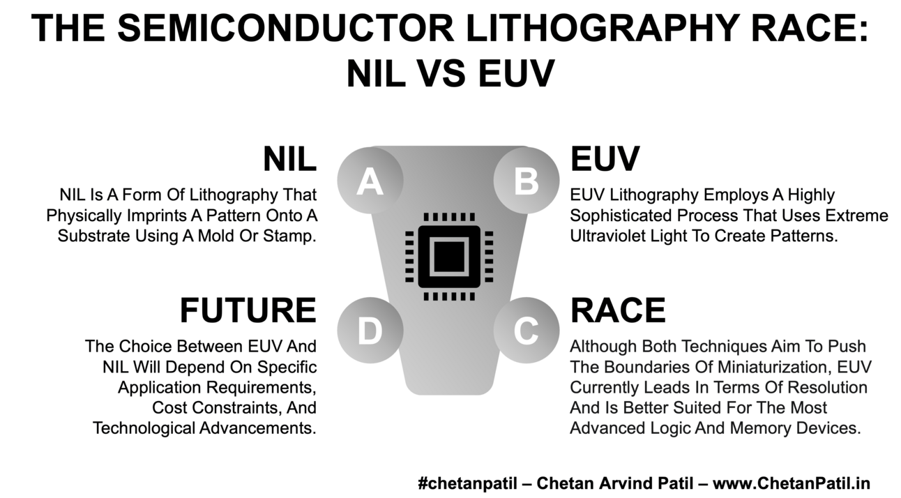
In semiconductor manufacturing, lithography is a pivotal process. It involves transferring circuit patterns onto a silicon wafer, a foundational step in creating integrated circuits (ICs). Two of the most advanced lithography techniques currently at the forefront of this industry are Extreme Ultraviolet (EUV) and Nanoimprint Lithography (NIL). Nanoimprint Lithography (NIL) and Extreme Ultraviolet Lithography (EUV) are two technologies used in semiconductor fabrication, each with advantages and challenges. Below is a comparative analysis.
Extreme Ultraviolet Lithography (EUV):....

THREAD
Semiconductor manufacturing process is not only very complex but also requires lot of investment due to several different types of equipments and facility requirements. Watch this information video and learn about how different process steps eventually lead to creation of FET devices.
Finding the first semiconductor job could be a daunting task. It not only requires specific educational qualification but the profile should also match the industry requirements. If you are a student (or know a student) looking to enter the semiconductor industry as a professional, then read this informative steps on how to setup the profile needed for the semiconductor industry and launch the semiconductor career swiftly.
Generating semiconductor research ideas is slowly becoming a challenge. Students focusing on semiconductor research thus could find a way forward by exploring different semiconductor roadmaps. Which then could recently open avenues to new types of research ideas. As these roadmaps focus both on the technical and business gaps along with the opportunities.
LLM powered silicon design is going to be a game changer for the semiconductor industry. It could drastically reduce the time to tape out along with the ability to bring errors to near-zero. This can massively reduce the cost of developing new silicon chip and thus helping the semiconductor companies with better ROIs.
As the SoC developing companies inches towards 1nm, the More Than Moore (MtM) solutions are rightly getting the needed traction. Some of the promising MtM solutions are Wafer-Scale Engine (WSE), Chiplets with RISC-V, Tensor Processing Units and PIM SoCs.
VLOG
Watch the insightful video on how Semiconductor Package Engineering is and what the engineers work on.
Semiconductor Package Engineering is a specialized field within electronics and material science focused on the design, development, and production of semiconductor packages. These packages are essential components in electronics, providing mechanical, thermal, and electrical support for semiconductor devices like microchips and transistors. A package engineer's primary role is to ensure the integrity and performance of these packages, making them crucial in developing electronic products, from smartphones to computers and automotive electronics.
The educational qualifications for a semiconductor package engineer typically include a bachelor's degree in electrical engineering, materials science, mechanical engineering, or a related field. Some positions may require a master's degree or specialized training in semiconductor packaging. Continuous learning is also a vital aspect of this career, as the field is rapidly evolving with new technologies and materials. Professionals often attend workshops, seminars, and conferences to stay updated with the latest trends and advancements in semiconductor packaging.
Career options for semiconductor package engineers are broad and promising. They can work in various industries, including consumer electronics, automotive, aerospace, and telecommunications. Opportunities exist in research and development, where engineers can innovate new packaging solutions, as well as in production and quality assurance roles. As technology advances, the demand for skilled package engineers will grow, offering a challenging and rewarding career path for individuals with the right blend of technical expertise and creativity.
GOVERNMENT
UK government-backed incubator ChipStart launched for semiconductor chip startups. ChipStart is a two-year pilot programme backed by the UK government providing startups with technical and commercial support to help them bring new products to market.
Australian Strategic Policy Institute has released a report on how it is crucial for Australia to focus on semiconductor manufacturing and the ways in which the securing semiconductor talent is going to set it apart.
India's Gujarat state government has a dedicated semiconductor policy to attract investment in the semiconductor sector (mainly manufacturing) to attract FDI in semiconductor design and manufacturing. With Micron's upcoming assembly, pack and test factory in Gujarat, the state has already taken the lead forward with other states also gearing up to come up with more attractive state level policies.
Europe to double its global market share for semiconductors to 20 percent by 2030. The goal is for Europe to double its global market share for semiconductors to 20 percent by 2030 by utilizing the remarkable 43 billion euros that have been made available from the EU budget and private sector funds.
Germany has approved stakes by Bosch, Infineon and NXP in TSMC chip plant.
EU has identified semiconductor as one of the critical technology as part of a list of 10 critical technologies it aims to protect in a bid to bolster economic security amid increasing concerns.
US state of Oregon is looking for more funding from the legislature to help the semiconductor industry become a larger part of the state’s economy.
INDUSTRY
Canon’s nanoimprint technology (NIL) to cost a fraction of ASML's. NIL is going to be a game changer for the semiconductor industry, where the cost of manufacturing is doubling every year with major reason being the process technology needed the most advanced, complex and costly equipment. Canon's solution brings a breath of fresh air and can change the semiconductor photolithography segment forever.
Lam Research plans to set up a semiconductor lab in India's Karnataka state. The US-based semiconductor equipment and services provider is planning to invest Rs. 236 as part of this lab and also aims to support the development of Indian suppliers by establishing links with the existing supplier ecosystem in Karnataka.
Rohm Semiconductor is planning to produce silicon carbide (SiC) wafers for the first time within Japan in 2024 to expand its production capacity and increase supply stability. Rohm will manufacture 8-inch (200mm) silicon carbide wafers in its second factory in Miyazaki Prefecture, Japan, primarily for Rohm's internal use. The operation is expected to commence in 2024.
Intel might be on its way to get the big funding as part of developing U.S. defense chip facility This could greatly help the Intel's Foundry Services business and also boost Intel's growth.
Intel on other side has decided to shelve its plans of chip operation expansion in Vietnam, due to the concerns about the stability of power supplies and excessive bureaucracy.
Cadence Design Systems has decided to offers academia an open source 130nm SkyWater PDK. This could help students and researchers speed up the learning and research activity.
Amdocs and NVIDIA have formed a collaboration to accelerate the adoption of GenAI in the Telecom industry. Amdocs and NVIDIA will customize enterprise-grade LLMs running on NVIDIA accelerated computing as part of the Amdocs amAIz framework. The collaboration will empower communications service providers to efficiently deploy generative AI use cases across their businesses, from customer experiences to network provisioning.
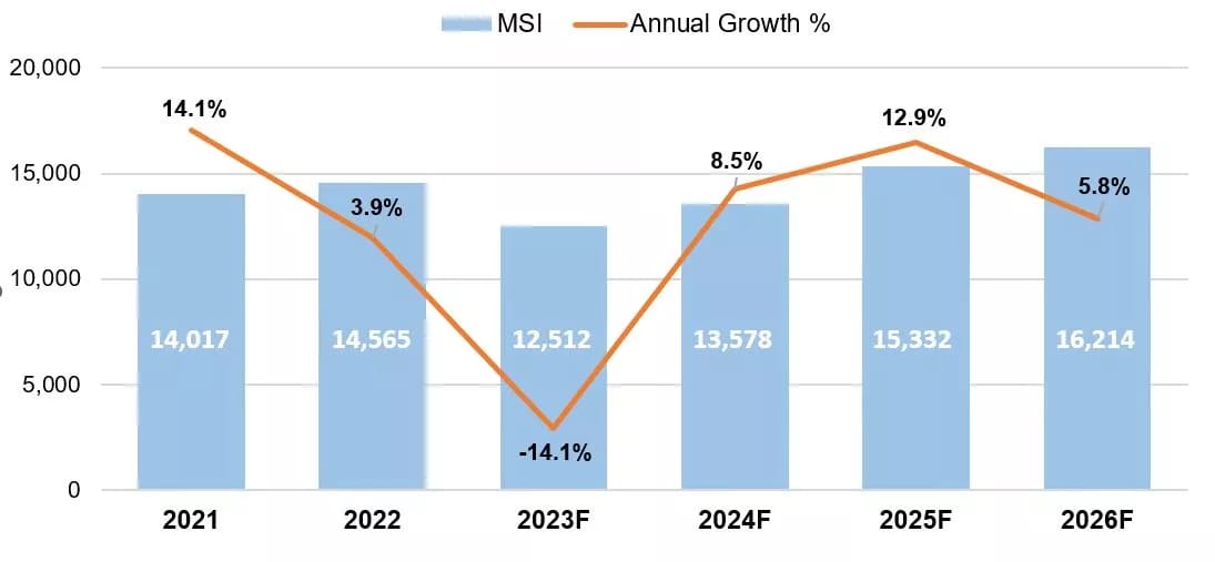
SEMI is expecting the global silicon wafer shipment to bounce back in 2024, after 2023 decline. Global shipments of silicon wafers are projected to decline 14% in 2023, to 12,512 million square inches (MSI) from the record high of 14,565 MSI in 2022 before bouncing back in 2024 as wafer and semiconductor demand recovers and inventory levels normalize, SEMI reported today in its annual silicon shipment forecast.

ACADEMIA
The University of Arizona and Arizona Commerce Authority (ACA) today announced an expansion of the Micro/Nano Fabrication Center (MNFC) located in the University’s Department of Electrical & Computer Engineering building in Tucson, Arizona. The ACA’s investment is part of a $100 million commitment announced last year to increase semiconductor and microelectronics development in the state. The investment will support technological development and further grow the skilled workforce to support advanced fabrication industries.
Delft University of Technology researchers have created a novel material that has a yield strength ten times higher than Kevlar, rivaling the strength of other super strong alternatives such as graphene and diamonds.The new material is called amorphous silicon carbide (a-SiC) and could have a host of applications that go beyond protective gear to enabling highly sensitive microchips.
RESEARCH
Columbia University scientists have recently discovered a new semiconductor material that is claimed to be the fastest and most efficient. This material is composed of one of the rarest elements found on Earth. However, the researchers believe they can find other more abundant materials that can operate at comparable speeds.
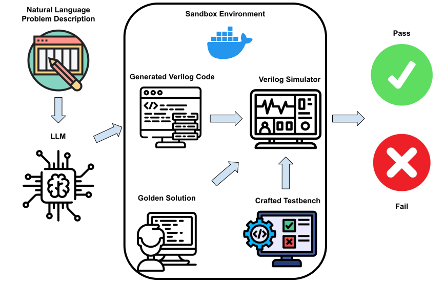
NIVIDIA GenAI research team have revealed VerilogEval: Evaluating Large Language Models for Verilog Code Generation. A LLM for silicon verification. Per NVIDIA's research team, "The increasing popularity of large language models (LLMs) has paved the way for their application in diverse domains. This paper proposes a benchmarking framework tailored specifically for evaluating LLM performance in the context of Verilog code generation for hardware design and verification. We present a comprehensive evaluation dataset consisting of 156 problems from the Verilog instructional website HDLBits. The evaluation set consists of a diverse set of Verilog code generation tasks, ranging from simple combinational circuits to complex finite state machines. The Verilog code completions can be automatically tested for functional correctness by comparing the transient simulation outputs of the generated design with a golden solution. We also demonstrate that the Verilog code generation capability of pretrained language models could be improved with supervised fine-tuning by bootstrapping with LLM generated synthetic problem-code pairs."

TOOLS
Trending Papers is a project that aims to organize computer science research in a logical, simple, and easy-to-follow way. It is designed to help you find what's worth reading first.
ChipsHub is a central place with access to a variety of expert-level tools that can be used in the chip design process. Spend your time working rather than struggling with code installation.
JOBS
Taiwan is looking to hire at least one lakh Indian workers in various sectors, including factories, farms, and hospitals as early as next month, according to a Bloomberg report. The two nations are anticipated to sign an employment mobility agreement by December, reported Bloomberg.
This could be an unique opportunity for students in India, who can get trained at some of the World's top semiconductor manufacturing facilities and later on can also enable development of similar ecosystem in India.
CONNECT
Whether you are a student with the goal to enter semiconductor industry (or even academia) or a semiconductor professional or someone looking to learn more about the ins and outs of the semiconductor industry, please do reach out to me.
Let us together explore the world of semiconductor and the endless opportunities:
Website: https://www.ChetanPatil.in
Twitter: https://twitter.com/iChetanPatil
Instagram: https://www.instagram.com/ChetanArvindPatil

